Design for Manufacturing
Lead: Bhaskar Choubey
Bhaskar’s team aims to establish rule-based strategies for thin film device manufacturing and identify system circuit configurations for coping with variability for truly wearable systems.
They will also study the lifetime failure of functional devices. Discussions started with Harish’s display, Moritz’s solar cell and Martin’s sensor development specialists to see when they will reach a certain maturity with their devices for the engineering team to pick up the devices for testing and modelling their variability and reliability.
Design of circuit configurations
Modelling
Large scale to atomic scale
Modelling – large-scale and atomic scale variations
Lead: C. David Wright
Reliability of thin film processes is poorly understood, thus David’s team needs to identify design guidelines to obtain acceptable performance for functional wearables. Santiago visited Oxford in Nov-Dec 2015 and studied the design of phase change devices. Gino is looking at atomistic simulations of materials and behaviour, concentrating first on the thermoelectric devices.

RESEARCH SCOPE
Sensors
Lead: Martin R Castell
Industrial Mentor: Matthew Brookes, dstl
Martin’s team works on electrochemical sensors based on organic thin films, which yet lack the necessary sensitivity and selectivity. Krishnan is developing an electrical percolation network of conducting organic lattices and aiming to differentiate the percolation region for interdigitated electrodes with a range of gaps. The task is the electrochemical polymerisation of PEDOT on interdigitated electrodes to create a percolation network followed by extensive characterisation.
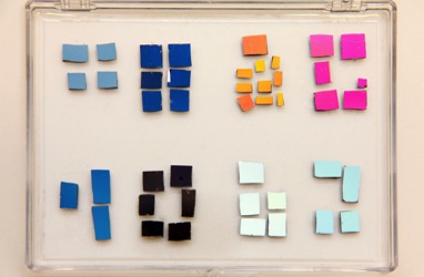
Some of the colourful samples
Flexible Display
Lead: Harish Bhaskaran
Industrial Mentor: Bodle Technologies Ltd.
Harish's team works on creating next-generation display technologies based on SRD (Solid-State Reflective Displays) on flexible substrates. Given that the basic thin films were proven on mylar substrates the team's goals are to understand how devices can now be made using this technology on flexible substrates.
Thermoelectric Energy Harvesting Module
Lead: Dan Hewak
Dan’s team is developing a thermo-electric module, complementing the organic photovoltaics as a secondary energy source. Flexibility limits the substrate material choice. The team successfully deposited BiSbTe and BiTe thin films by RF sputtering on polyimide at temperatures below 200C. Demonstrated p-type and n-type Ga:La:S thin films and reported on feasibility in thermoelectric devices.
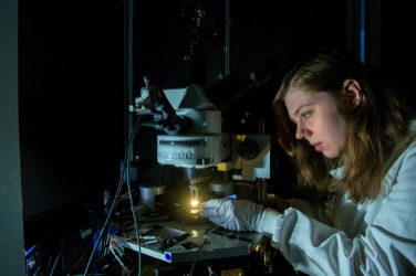
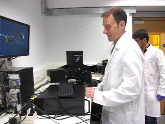
Probe station for thin film characterisation
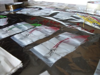
PEDOT interdigitated electrode devices connected to wires and ready for test
Organic Photovoltaic Energy Harvesting Module
Lead: Moritz Riede
With active layers of only hundreds of nm, and processing on thin plastic films, organic photovoltaics are highly compatible with wearable and flexible electronics. Moritz’s team needs to tailor OPV modules to the voltage requirements of other components as needed for integrated wearables. The challenge is the integration of 6-8 layers of advanced OPV modules. Sameer began cataloguing of module design based on voltage and power requirements of functional devices, and developing CAD layouts of various device geometries.
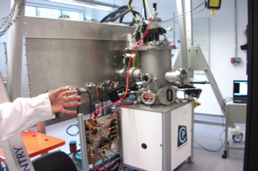
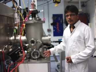
Vacuum deposition tool
Ex-situ Metrology and Characterization
Lead: Harish Bhaskaran
Harish and Jeremy worked on cross sectioning of components and carrying out electron microscopy to indicate aspects such as interfacial failures: delamination, electromigration, oxidation. Jeremy used electron microscopy and aberration corrected TEM and observed that Ge segregating to the interface is the failure mechanism.
Process Control for Waste Reduction
Lead: Moritz Riede
Monitoring of material usage for each deposition was started, building broader database for material usage. The relationship between material usage, processing conditions and device performance should be obtained to improve process control and mechanical design.
Operating the vacuum deposition tool
Photovoltaic measurements
In-situ Metrology Solutions for Thin Film Manufacturing
Lead: Moritz Riede
Moritz and Sameer procured and installed advanced metrology tools: the Woollam R2 spectroscopic ellipsometer and reflectometer. It was integrated to the upgraded vacuum chamber for in situ monitoring of thin film deposition.
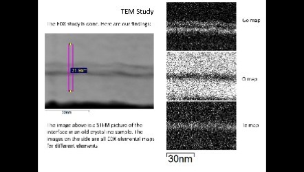
STEM imaging showing potential segregation of Ge
Device Fabrication using Roll-to-Roll on Flexible Substrates
Lead: Hazel E. Assender
Thin film deposition of the various materials options will be designed and implemented on Oxford’s roll-to-roll vacuum webcoating facility.
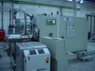
Richard and Clara enhanced the webcoating equipment in Begbroke for optimal device layers depositions. It is suitable for evaporation of metals and organic materials, polymer deposition and sputtering. The ultimate aim is to investigate integration of multiple layer structures within a manufacturing facility to build test devices in a roll-to-roll manufacturing environment.
Facilities at CPI for roll-to-roll ALD deposition will be used for barrier and, if appropriate, device active layers.
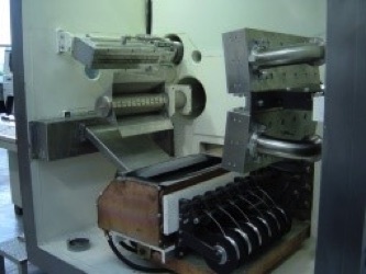
Various rolls inside the R2R tool
Roll-to-Roll Deposition Tool in Begbroke Science Park
Roll-to-Roll Process Development
Lead: Hazel E. Assender
Hazel works closely with all the other teams to help key in on the metrics for process development on roll-to-roll machines. The concept here is to make sure that processes developed even at a device level are evaluated with an eye towards how they can me made compatible with any eventual R2R production.
Flexible Components
Metrology
Modelling and Design
Manufacturing